Trace: » group1start
Weekly Reports
Topic selection
Traffic monitoring system
Design
Proof-of-principle
Final Reports
1.Project Objectives
The original objectives of this project were to construct a traffic monitoring system. The system was required to use optics to measure the velocity of both automobiles and pedestrians on a quiet street, count the number of each that pass through the system, and keep a log of the data. Later in the project development, these objectives were altered to include only pedestrians. The system was intended to work under all normal environmental conditions such as rain, snow, and of course, in daylight. The system could not pose any threat to the health and safety of those who entered it. The project was limited to a budget of $200 CDN for all component and construction costs.
2. Final Design
The final design consisted of four subsections that combined to produce a system: the optical system, the modulating circuit, the comparator circuit and the microcontroller system.
2.1 Optical System
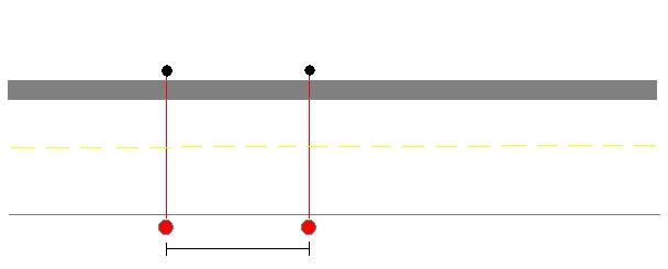
In the optical design, infrared light was chosen over visible light because longer wavelengths are less likely to be scattered due to Rayleigh scattering and therefore can be transmitted farther. Infrared light also experiences less ambient interference from the sun because the spectral flux of the sun is smaller in the infrared region[1]. The final design consisted of two collimated infrared LEDs, approximately 1m apart, directed across the hallway, at waist level, to two infrared receivers in the following configuration:
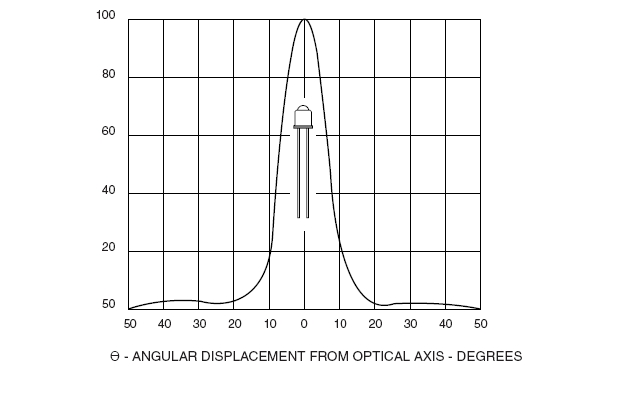
Infrared LEDs with a small emission angle were required for this application to reduce beam divergence. Diverging beams would interfere with the other receivers, and a highly diverging beam may be wider than a person, making the system ineffective. For this reason, an infrared LED (wavelength 935-955 nm) with an emission angle at half power of eight degrees was selected; Digikey model number 1N6264. The typical emission pattern of this LED is shown below.[2]
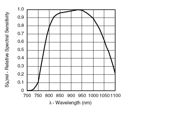
The wavelength range of the LED was chosen based on the pre-selected receiver; Digikey model TSOP852. As can be seen from the spectral sensitivity graph below[3], the wavelength of the LEDs corresponds to the highest possible receiver sensitivity.
The receiver was selected primarily for its high immunity against ambient light, such as fluorescent lights and, most importantly, sunlight. The receiver uses two lenses with an epoxy cap that acts as an infrared filter, cutting out almost all unwanted light. The two lenses increase sensitivity and receiving angle. While it is desirable for the LEDs to have a very small angular displacement, it is important that the receiver’s receiving angle is not too small, as this will make alignment nearly impossible. At the same time, in this application, if the receiving angle is too large the receiver may pick up signals from neighbouring LEDs, causing errors. The chosen receiver has a fairly large receiving angle of 50 degrees; however small blockades such as pieces of cardboard placed beside the receivers are effective at blocking out unwanted signals from neighbouring LEDs.
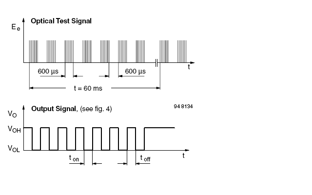
The receiver attains its extremely high insensitivity to ambient light by distinguishing between data and disturbance signals according to their carrier frequency, burst length and envelope duty cycle. The TSOP852 model is configured as a bandpass filter centred at 38kHz. However, to further decrease ambient interference, the receiver will not accept any continuous signal, even those at 38kHz. This feature effectively blocks out all ambient light sources, including fluorescent lights and sunlight. In order for the intended signal to be detected as discontinuous, the 38kHz carrier frequency must be contained within an envelope where the signal ‘burst’ of 38kHz signal must be between 10 and 70 cycles long, and for each burst there must be a minimum rest period of 10 cycles. This required the LEDs to be modulated using a 555-timer circuit. The receiver outputs a digital high signal during the rest periods, and a digital low during the ‘burst’ cycle, as shown in the figure below[4].
When the signal is blocked, the receiver detects a very long rest period, and therefore the output of the receiver output is digitally high for the duration that the beam is blocked.
[1]Spekkens, Kristine. “How do we know that sunspots are associated with the Sun's magnetic field?” Ask an Astronomer, http://www.thermalphysics.org/graphics/sun.jpg (accessed September 12, 2008).
[2]1N6264 Datasheet, Fairchild Semiconductor. http://www.fairchildsemi.com/ds/1N/1N6264.pdf. (accessed September 2008).
[3]TSOP852 Datasheet, Vishay Semiconductors, http://www.vishay.com/docs/81764/tsop852.pdf (accessed September 2008).
[4] Ibid.
2.2 Modulated Frequency Generator Circuit (MFGC)
The MFGC is the sub circuit which effectively modulates the infrared light to be received by the receiver. It was interpreted at first that the receiver could comprehend a constant flow of 38kHz modulated light, however upon further examination of its specifications sheet, it was observed that the light needed to exist within an envelope frequency that was high for the equivalent time of anywhere between 10 and 70 pulses of 38kHz light, and low for a minimum of time of 10 pulses of the same light. The modulated input that needed to be produced can be observed in the previous figure.
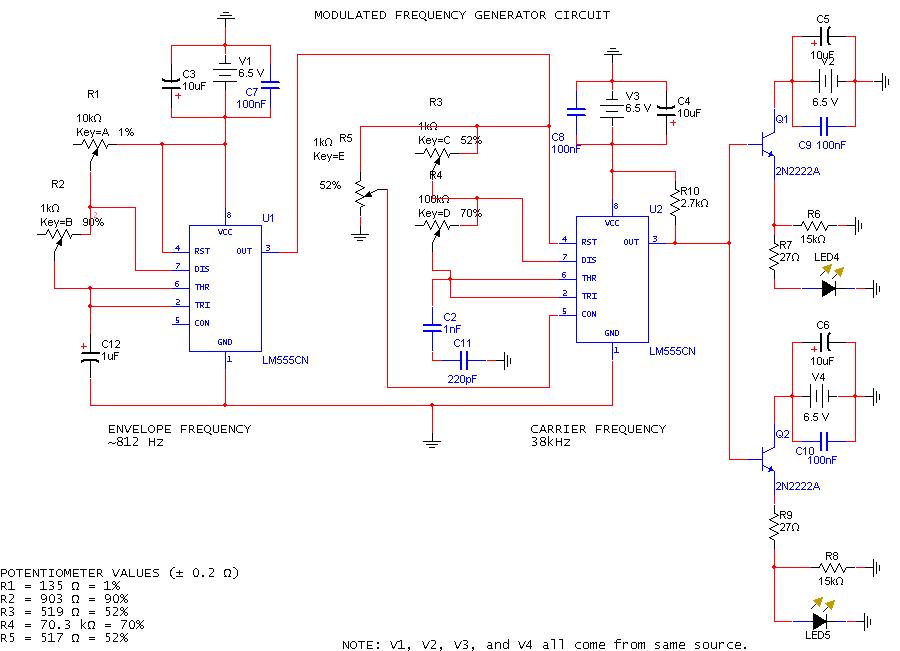
The ultimate responsibility of the MFGC is to modulate the light to produce a similar output as observed above. To accomplish this, the use of two 555-timer astable multivibrator circuits was necessary. An astable multivibrator oscillates between two stable states; in this case these was a positive voltage of about +6.5V and a voltage of 0V. The +6.5 comes from the option to use four AA batteries to power the circuit, each with a voltage of +1.5V. See below for the MFGC schematic.
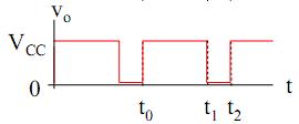
As observed above, the first stage of the MFGC creates the envelope frequency required by the IR receiver as mentioned above. The carrier frequency of 38kHz is created by the second stage of the amplifier. The frequency output of each of the stages is determined by the resistor combinations R1 and R2 for the first stage, and R3 and R4 for the second stage. R5, present on the second stage, is responsible for trimming the rise and fall time of the 38kHz output, so that it creates steeper rise and fall times, essentially making the square wave more square-shaped and less slanted. For calculation of the frequencies in each stage observed in the MFGC, analysis of the general output of an astable multivibrator was required (See Below).
Where t1-t0 is the time that the output is high, and t2-t1 is the time that the output is low, and Vcc is the supply voltage – this is +6.5 volts in this case. These times are calculated using the following formulae:
(1) t1-t0 = (Ra + Rb)(C)(ln2)
(2) t2-t1 = (Rb)(C)(ln2)
Where RA and RB are resistors R1 and R2, and R3 and R4, for the first and second stages, respectively. C is the capacitor observed at C12 for the first stage and C2 for the second stage in the MFGC.
In the case of the envelope frequency, the time that the output is high, given by equation (1), was found to be 7.19E-4 s, which is equivalent to the time taken for about 51 pulses of 38kHz light to pass. The time determined by equation (2), or the low time, was calculated to be 6.26E-4 s, or the equivalent time of 24 pulses of 38kHz light low. Thus, the envelope allowed for 51 pulses of 38kHz light to be output, with a rest time equivalent to the length of time needed to output 24 pulses. As the 51 pulses high was within the 10 to 70 pulse window, and the 24 pulses low was greater than the minimum 10 pulse rest time, it was evident that this circuit would allow for a proper output. The resistor values at R1 through R5 were all designated as potentiometers so that both the envelope and the carrier frequencies can be tuned to their precise windows of operation. Fixed resistors could have changed their resistances through excessive testing as well as temperature changes in the external environment, however with potentiometers, if any changes in resistance were to occur due to the previously mentioned factors, each potentiometer can be adjusted until the desired wave form is recovered. Thus to ensure optimal success of creating the two necessary frequencies, it was justified to use potentiometers. The capacitor values attached to each stage were arbitrarily chosen and the subsequent potentiometer values were adjusted based on these selections.
The final output through the second stage and into the LEDs was used to bias the base of two NPN BJTs to allow for maximum voltage and current flow into the LEDs to increase their output intensities. The use of a 2.7kΩ “pull-up” resistor was necessary to add current to the output signal for better biasing purposes, while the 15kΩ “pull-down” resistors were used to limit the voltage into the LEDs so that they did not burn out. The voltage sources contained both two capacitors surrounding them as to negate the effects of any transient AC ripple voltages coming from the DC input of +6.5 volts. This ensured a clean DC supply was powering the circuit.
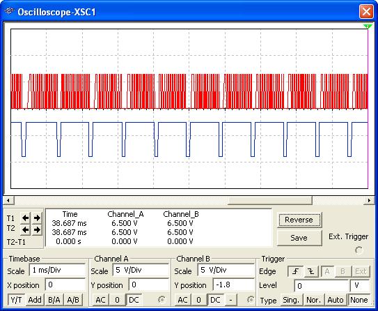
The simulated output of the MFGC can be observed in the following figure, and echoes the test input for the IR receiver, observed as the “Test Output” figure above. Note that the red signal is the modulated output of the second stage which exits through the LED, and the blue signal is a measurement of the envelope frequency, which outlines the groups of 38kHz pulses in the red signal.
2.3 Comparator Circuit as Receiver/Demodulator
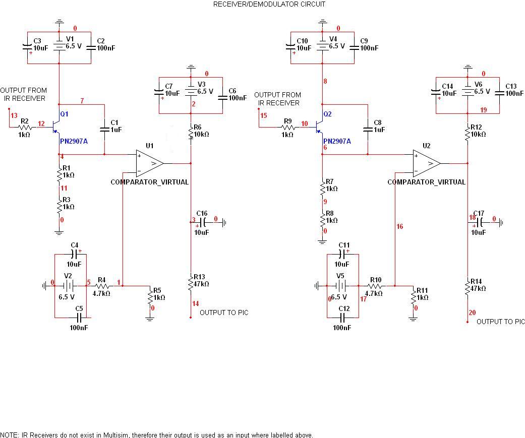
This sub circuit contains the IR receivers which receive the modulated light from the MFGC. The output of the IR receivers can be observed in the second half of theoretical output diagram above defined by the IR receiver, where it is observed that for the time that the envelope frequency is high, the output of the receiver is low, and for the time that it is low, the output of the receiver is high. The output of the IR receivers is essentially a square wave with a high pulse equal in magnitude to the low pulse of the envelope frequency of the MFGC. The RDC can be observed in the following figure.
The square wave output from the receivers were too difficult to analyze within the microcontroller. Therefore the addition of the demodulator circuit was necessary in the later creation time of the project. The demodulator circuit, observed above as a PNP BJT, a 1μF capacitor, two 1kΩ resistors, and a comparator, acts to change the square wave output into a constant high voltage. Initially, if the beams were to be blocked, the square wave output would merely change frequency, however, with the addition of the demodulator circuit, the final output into the microcontroller would be a constant high voltage which only dropped low if the beam were to be blocked. This allowed for much simpler analysis.
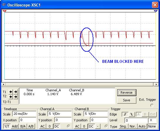
To convert the square wave into a constant high voltage, the demodulator circuit takes the square wave and biases the BJT. Upon doing this, the capacitor is able to charge and discharge periodically within a given voltage window. This capacitor wave form is fed into the positive input of the comparator. In the negative input, a threshold, constant DC voltage is applied. When the circuit is not blocked, the wave form of the capacitor does not drop below the threshold voltage and therefore the output of the comparator remains high. Once the beam is crossed, the capacitor wave form drops below the threshold and causes the output of the comparator to switch to low. This is illustrated in the following figure.
The jagged wave form in the above figure is the output of the capacitor which is the first input of the comparator. The second input of the comparator is the observed DC voltage at roughly +1.14 volts. Upon crossing the IR beam, the square wave output of the receiver changes frequency, which in turn causes the capacitor to discharge below the previously mentioned threshold voltage. At this point the output on from the comparator switches from high to low. This corresponding output can be viewed as follows.
 Receiver Output to Microcontroller
The output seen above is placed into the input of the microcontroller. It is a constant high output until the beam is blocked, where it switches to low. This event is much more easily analyzed by the microcontroller than the square wave. The demodulator circuit is replicated for the second IR receiver output. The comparators used were actually part of a quad comparator integrated circuit provided by Glen Leinweber.
Again, the DC sources have filter capacitors on them to remove any transient AC ripple voltages. Four AA batteries are used to power this circuit as well.
2.4 Microcontroller System
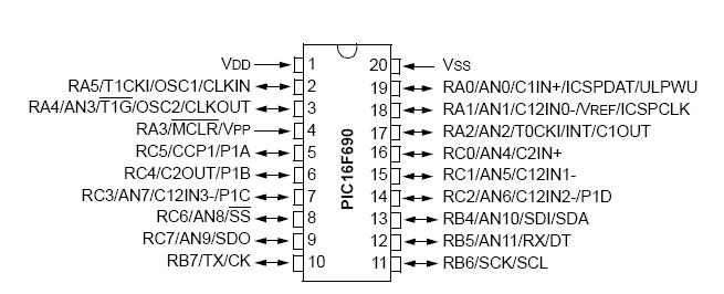
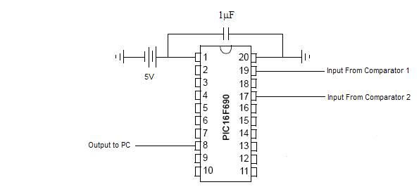
The 20-pin 8-bit PIC16F690 microcontroller was selected for use in the final design. The key features of the PIC for this design were the interrupt-on-change feature in Port A, and the timer1 overflow interrupt, both of which will be described below. The microcontroller also contained an internal clock and inverter, reducing external components and greatly simplifying the microcontroller circuit. This PIC was easier to work with and debug compared to larger PICs considered for the design. The pin and circuit diagrams can be seen below [1].
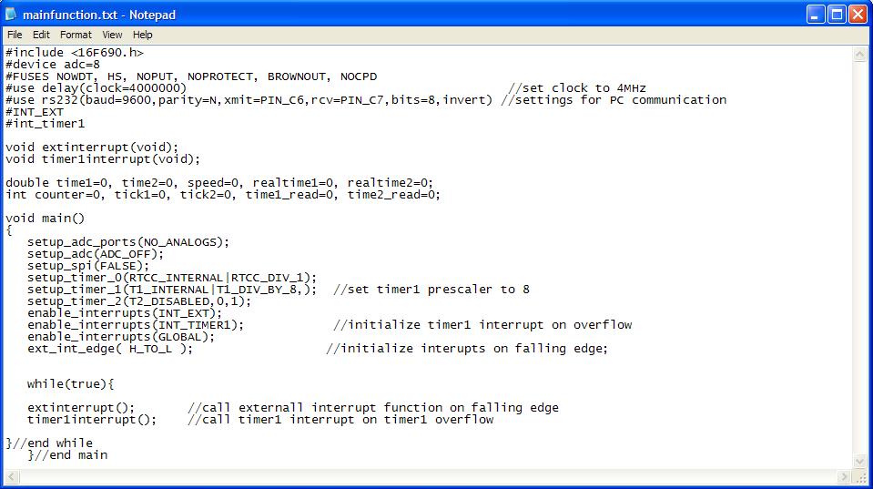
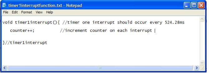
The final code was designed in accordance with the modified scope, therefore it assumed that the object was a pedestrian, and under this assumption could determine their speed and direction, and log the data into a text file. The program works in the following manner: Within the main function there are two interrupts: ‘timer1interrupt’ and ‘extinterrupt’. An interrupt is a function outside of main that is called only under specific circumstances. ‘Timer1interrupt’ is called whenever timer1 overflows, and ‘extinterrupt’ is called every time there is a falling edge, as seen in Figure 8. Timer1 was programmed to increment once every eight microseconds by setting the internal clock to 4Mhz and the prescaler to 8. A prescaler of eight indicates that the clock will increment once every 32 cycles [2].
Time in increment= [increments per cycle]/ [frequency]
               = [32 increments/cycle] / [4,000,000 cycles/s]
               = 8ms
Timer1 calls an interrupt every time it overflows, which is every 65,535-clock increments for a 16bit timer. This means that timer1interrupt will be called every 524.26ms.
Timer1 interrupt time= [time per increment] x [increments to overflow]
		          = [8ms/increment] x [65,535 increments]
		          = 0.52428s
		          = 524.28ms
Each time ‘timer1interrupt’ is called, an outside integer variable called ‘counter’ is incremented by one, so that each “tick” of ‘counter’ represents 524.26ms. Counter, being an 8-bit integer, will overflow when it reaches a count of 256, which corresponds to 134.21 seconds, or 2.24 minutes.
Counter overflow time= [time per increment] x [increments to overflow]
			=  [0.52428s/increment] x [256increments]
			= 134.22s
			=2.24 minutes
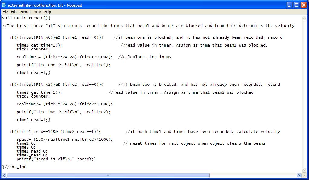
Upon re-examination this was an error made in the code since if the first beam were to be blocked before rollover, and the second after, the direction and speed calculated would be incorrect. However, when the final code was implemented, the rollover appeared to be happening much more often than it was programmed to, closer to every two seconds than every two minutes. The cause of this malfunction is due to an error in either the clock or timer settings, however the exact source within the code is unknown. ‘Extinterrupt’ was programmed to interrupt whenever a falling edge was detected in either of the input pins. Pseudocode for the interrupt follows:
- if pin A0 is low and a time1 has not been recorded, record and output time1
- if pin A2 is low, and a time2 has not been recorded, record and output time2
- if both time1 and time2 have been recorded calculate velocity using 1metre/(time1-time2)
- reset time1 and time2 to zero and ‘unrecorded’
- output velocity
A trial version of CCS PCW C Compiler was used to compile the code, and the PICC C Plus program available in the lab was used to program microcontroller. The segmented code can be seen in the figures below.
[1]PIC16F690 Datasheet, Microchip, http://ww1.microchip.com/downloads/en/DeviceDoc/41262E.pdf (accessed September 2008).
[2]Dubuc, Martin. “Programming Tips.” http://mdubuc.freeshell.org/Robotics/Tips.html (accessed October 2008).
3. Proof-of-Principle Tests
3.1 Optical Proof-of-Principle
The first part of the proof of principle test conducted was to detect a strong signal from a 38kHz modulated LED from a distance of 20ft. The tests were conducted in ambient light sources in order to imitate the ambient light of the sun that will be encountered outside. The LED was modulated according to the receiver specifications (38kHz, 70 cycles on, 10 cycles off) using two function generators. The second part of the proof of principle test was to block the signal and ensure that the system could detect the blockage and redetect the signal once the object had been removed from the beam path.
The IR receiver successfully detected a modulated signal from the LEDs from 20ft away, though this distance could be increased if necessary. Optical alignment was a sensitive procedure, which was improved with the addition of collimating lenses. Once aligned, the mechanism worked perfectly without fault, with the receiver able to distinguish between a blocked and unblocked signal for every trial. Tests with multiple oscilloscopes deemed that the response time of the receiver was negligible.
Given that the signal was easily detectable from 20ft in an environment with high levels of ambient light, the proof of principle test results demonstrated that the optical system was feasible, provided that the modulation of light accomplished using function generators was reproducible using the proposed modulation circuits.
3.2 Electronic Proof-of-Principle
The initial electronic PoP consisted of a multisim simulation of the MFGC and receiver circuit, and an explanation of the microcontroller. As the parts for the circuit had not arrived yet, the analog portion had not been built and the programming of the microcontroller was still in development. An explanation of the interrupts was given for the microcontroller and how they would be used to observe when the beam was blocked. However, this was under the assumption that a square wave input would be used for the microcontroller, and not the simpler DC signal. Thus, it was too difficult to implement all the ideas in the electronic PoP as later modifications to the circuit proved that an entirely different microcontroller with new code would be used.
Given the chance to present later on, the completed MFGC circuit was demonstrated and powered with batteries to transmit an IR signal across the lab to be received and observed on an oscilloscope. This pseudo-PoP allowed the group to demonstrate that the analog components were able to be constructed in accordance with the Multisim schematic, and that it could be powered using batteries. Also, the microcontroller was programmed to output “Leigh”, indicating a beginning understanding on how to place code on the microcontroller and use it to perform operations. Overall, the electronic PoP mainly proved the validity of the then-existing circuit and microcontroller combination.
4. Final Completed Product Description
The MFGC, the RDC and the DPC as described in the final design can be observed in the following figures.
 Modulated Frequency Generator Circuit
 Comparator Circuit as Receiver/Demodulator
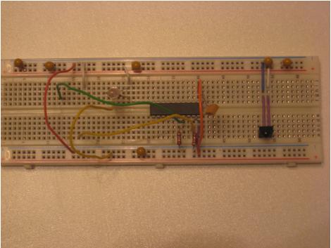
As observed in the above figures, the entire circuit fit onto five bread boards. In the figure depicting the RDC, it is important to note that the quad comparator is set to receive three inputs. This is due to the initial design of three beams. However since one of the receivers malfunctioned, only two of the inputs were used, however the third input with the corresponding third demodulator circuit, was left on the bread board. The output from the second stage of the larger circuit in the MFGC screenshot, is also used to bias the base of the BJT in the smaller circuit of the same diagram. Two separate IR receivers were used. One was the ordered receiver from Digikey. Originally, it did not function properly, as it lost its signal from time to time. However during the testing of it implemented with the demodulator circuit, it always kept a constant output when receiving a signal. The second receiver, observed in the DPC figure, comes from an old ENG PHYS 4A06 project, and also receives light modulated at 38kHz. A visible LED is present in combination with a parallel resistor in the above figure to allow for a voltage step down from the +6.5V supply, so that the microcontroller can be powered with about +5V without being damaged. Also note the numerous electrolytic capactiors present in all three circuits, used to filter out transient AC noise from the power supply.
5.Final Demonstration of Completion
5.1 Performance
The final product was tested in the lab, under ambient light conditions. The testing demonstrated that the project was successful at determining when a beam was blocked, which beam was blocked, and outputting the time of the block to the PC screen and text file. The project was also successful at implementing the speed calculations only after both beams had been passed in succession. There was, however, a problem with the timer within the microcontroller program. No solution was found to the rollover problem, and therefore a number of the speed calculations were inaccurate, due to the fact that the clock had rolled over in the time between the first beam being blocked and the second beam being blocked.
5.2 Objectives Met
Despite the microcontroller timer problems, many of the objectives of the design were met. The completed project met the following objectives:
- Able to detect when a beam was blocked.
- Able to determine which of the two beams was blocked.
- Able to record the microcontroller timer time when a beam was blocked.
- Able to use recorded beam blockage times and use them to calculate the speed of the pedestrian.
- System was fully portable for outdoor use.
- System was able to attach and function with any PC.
- System met all safety standards.
- System stayed within required budget.
5.3 Objectives Not Met
There was only one final design objective not met, and this was the ability of the microcontroller to run a timer without rollover for a long enough period to enable accurate time recordings and therefore output correct speeds. The rest of the microcontroller program functioned as intended. Unfortunately, the accuracy of the time recorded was instrumental to the speed calculation, and to the overall performance of the system.
6. Budget
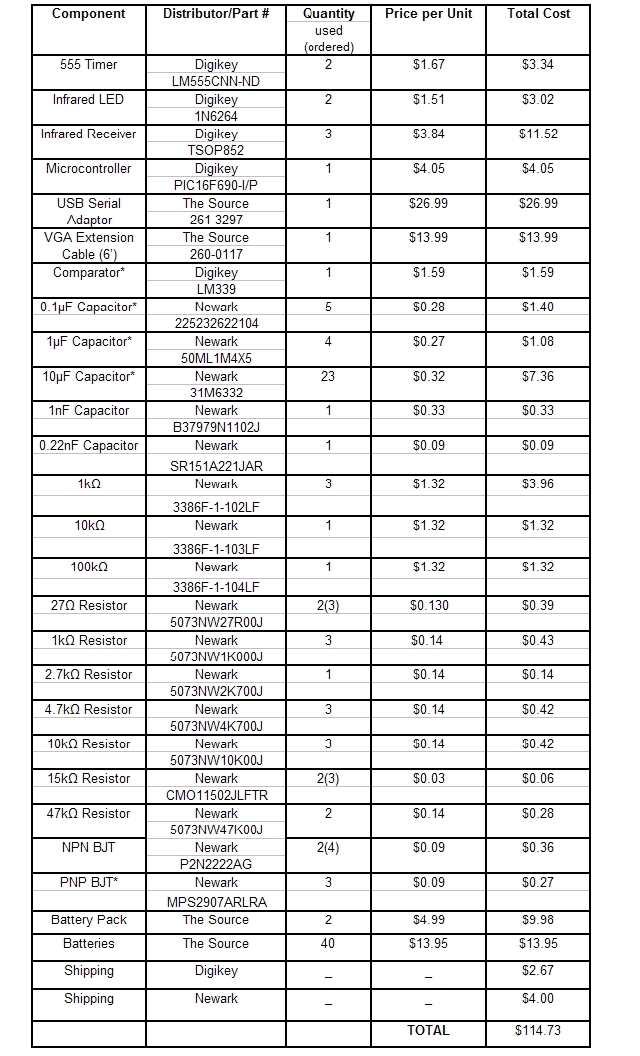
The allocated budget for the project was $200 CDN, including all component, construction and shipping costs. The following table is a comprehensive list of all components used in the completed product and their individual costs. Components that were used but not ordered are marked by an asterisk(*).
Parts Used
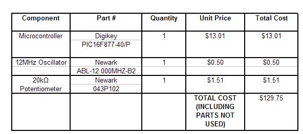
Parts Ordered But Not Used
The oscillator was purchased in anticipation of using it with the PIC16F877 microcontroller. The potentiometer was never utilized because a more applicable one was obtained from the Lab Technician. There was only one damaged part: a receiver was burnt during testing because it was put in the circuit the wrong way.
As shown in the tables and discussions above; the project stayed well within budget, including any components that were purchased but not implemented in the final design.
You are here: start » group1 » group1start

