Trace: » group3final
Eng Phys 3A03 Design Project
Final Report for Group 3 (Free Space Optics)
By George Montgomery, Owen Taggart, and Anthony Tsikouras
1.Project Objectives
The project is to create a free-space optical communication system. The system must be capable of sending text and images through free space between buildings, or similar distances. The project should not exceed $200 in cost of construction.
2.Initial Design
From the beginning, the concept was essentially the same: a laser used to send a signal (modulated by computer across a distance, where it would be received by a photosensitive circuit component, and reconstructed for the receiving computer. There are some notable decisions and changes that were made in the process, before the final design was established.
Receiving Structure
One of the greatest concerns of the project was beam alignment, which was a two-prong problem. First, the beam may be difficult to align over large distances, considering a typical photodiode or phototransistor has a receive area of maybe 1 mm^2. Second, the laser may not be visible in direct sunlight, and if the phototransistor is exposed, the direct sunlight could set it off, making the laser's signal lost. The first idea was then to purchase an ABS tube from a hardware store, and position a lens from a magnifying glass at one end. The phototransistor would then be mounted at the exact focal point of the lens, and so any normal incident laser beam that hit the lens would be directly focused onto the phototransistor. The laser pointer source would theoretically be far enough away to be seen as normal.
Unfortunately, theory does not work perfectly in practice: corrections were made to the phototransistor's position on a regular basis, possibly because the assumption of normal light was not obeyed, possibly because of aberrations on the $1 magnifying glass lens, and possibly because mounting the photosensitive spot of a phototransistor in the direct center of a round object is a challenge in itself. It quickly became evident that changes would need to be made on the receiving end for alignment, and the tube would not work for this.
Briefly, ideas of an openable 'cave' for the receiving area, so the phototransistor could be aligned while still preventing sunlight, were discussed. However, instead of scrapping the original pipe idea, the ABS pipe was modified to have a lifting panel of a hinge cut out at the receiving end. The lens in the pipe was not as important anymore, since alignment would still be required on the receive end regardless of whether or not the lens was present, but the lens doubled as a beam converger to fight the extreme divergence of some of the cheap laser pointers.
The main issue now was the alignment adjustments that needed to be made with a fair amount of precision. For this, a base would be made for the ABS pipe to sit on. Initially, this base was constructed from two slabs of Styrofoam with screws as legs, which could adjust the height at all four corners of the device. The base was makeshift from supplies in the lab, and was not sturdy (and made a terrible sound when the screws slid against the table).
Sending Structure
The laser's wavelength was decided early on. First, red lasers are very common, so, for the sake of the budget, the cheaper solution would be favored. At the same time, any infrared sources would be very difficult to align over long distances. Finally, most low-cost photodiodes and phototransistors, while designed to operate in the near-infrared around 800-900 nm, also have a fairly strong sensitivity to the 650 nm red light produced by low-cost diode lasers.
The method of mounting a laser in an adjustable manner was often overlooked in the project. During the development of the project in the lab, this was generally accomplished with a clamp, which provided some rotational movement for the laser, and books for the clamp to sit on if height were needed. The first actual solution for the project was the miniature tripod that was used in the final design.
PC Communication
The send and receive circuits were initially going to communicate with each computer by use of a programmable microcontroller. This would allow for faster transfers, since the microcontroller could partially interpret the incoming data before passing it to the computer. However, the microcontroller did not end up being the speed bottleneck of the design, which was slowed mostly by the phototransistor's rise time. Also, since the microcontroller would theoretically speed up the process by interpreting the laser modulated signal as characters before handing it to the receiving computer, it would not be useful for pictures, where speed was important. In the end, the simplest idea was a direct link to the RS-232 port from the send and receive circuits.
There was also the question of how to send and receive pictures. Originally, Hyperterminal would be used, which would be ideal since it came preloaded on all versions of Windows since 1995. Unfortunately, when sending a file such as a picture, Hyperterminal relies on being able to receive data back from the receiving computer, handshaking to make sure no bits were lost (known as full duplex). This would be impossible with our system, where one side could only send, and one side could only receive. The options were to either create a double of the send and receive circuit, so the handshaking could occur, or find/write other software that would send a picture without requiring handshaking (known as half duplex). The free program Realterm was discovered that allowed half duplex file transfer.
3.Final Design
This description refers to the design as it was actually completed and not as it was originally conceived; hence, final design. The free-space optical system designed by Group 3 is a computer-to-computer system. This allows for the user interface to be handled by the computers, simplifying design and allowing for better integration with existing hardware. After all, most people own a computer. The final design has four basic components: an optical transmission channel to send data over, transceiver electronics to convert between electrical data and optical signals, terminal software used by the computer to control the communication system, and the mechanical assembly on which the components are mounted.
Optical Design
The optical communication channel is very simple, since this is intended to be a short-range free-space optics system, and is almost identical in its final form to the original design. As this is only a demonstration system, it operates in a half-duplex mode. This means that the communication channel is one-way: one end can only send data, and the other can only receive. As such, only one receiver and one transmitter were needed.
An ordinary “dollar variety” 650 nm red diode laser pointer is used as a transmitter. This laser was chosen for its low cost, easy availability, and design simplicity. The red wavelength is also less strongly absorbed by the atmosphere than shorter wavelengths. The use of a laser also simplifies the optics of the transmission channel. If the design had used an LED source instead, collimating optics would have been required to shape the output into a focused beam capable of traversing a long distance.
Unfortunately, this type of laser pointer suffers from reliability issues as well as highly variable beam quality. A large number of backup and replacement lasers were purchased against the possibility of laser diode failure. In order to simplify alignment, and account for the poor quality (high divergence) of some of the laser beams, a basic positive lens was used to focus the light onto the photosensor. The lens selected was a “dollar variety” magnifying glass. This lens was selected due to its low cost, fairly large area, and easy availability. The photosensor is located at the focal point of this lens, which was experimentally determined to be approximately 34 cm from its center. The lens then directs a laser beam entering at a normal incidence to any portion of its surface onto the photosensor.
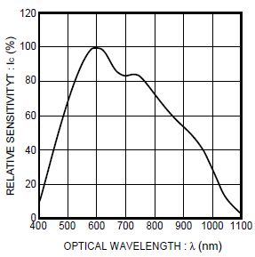
The photosensor is an RPM-075PT surface mount phototransistor from Rohm Co. Ltd. Phototransistors and photodiodes are light-sensitive semiconductors that use the energy of light striking the device to generate a small current, similar to a solar cell. The amount of current depends on the amount of light striking the active area of the device, the sensitivity of the device at that wavelength, and the electrical properties of the device. In this case, the phototransistor was chosen over the photodiode due to its incorporation of internal gain, which produces a much stronger current. The particular model used was originally selected because its peak sensitivity of 600 nm falls very close the 650 nm wavelength of the laser pointer, as can be seen on this graph taken from its datasheet:
The transistor was also found to a have a very strong optical response, producing voltage swings of as much as 4 Volts between laser on and laser off conditions. This, combined with the unfortunate disappearance of later phototransistors ordered to replace it, prompted the group to keep it in the project despite its shortcomings.
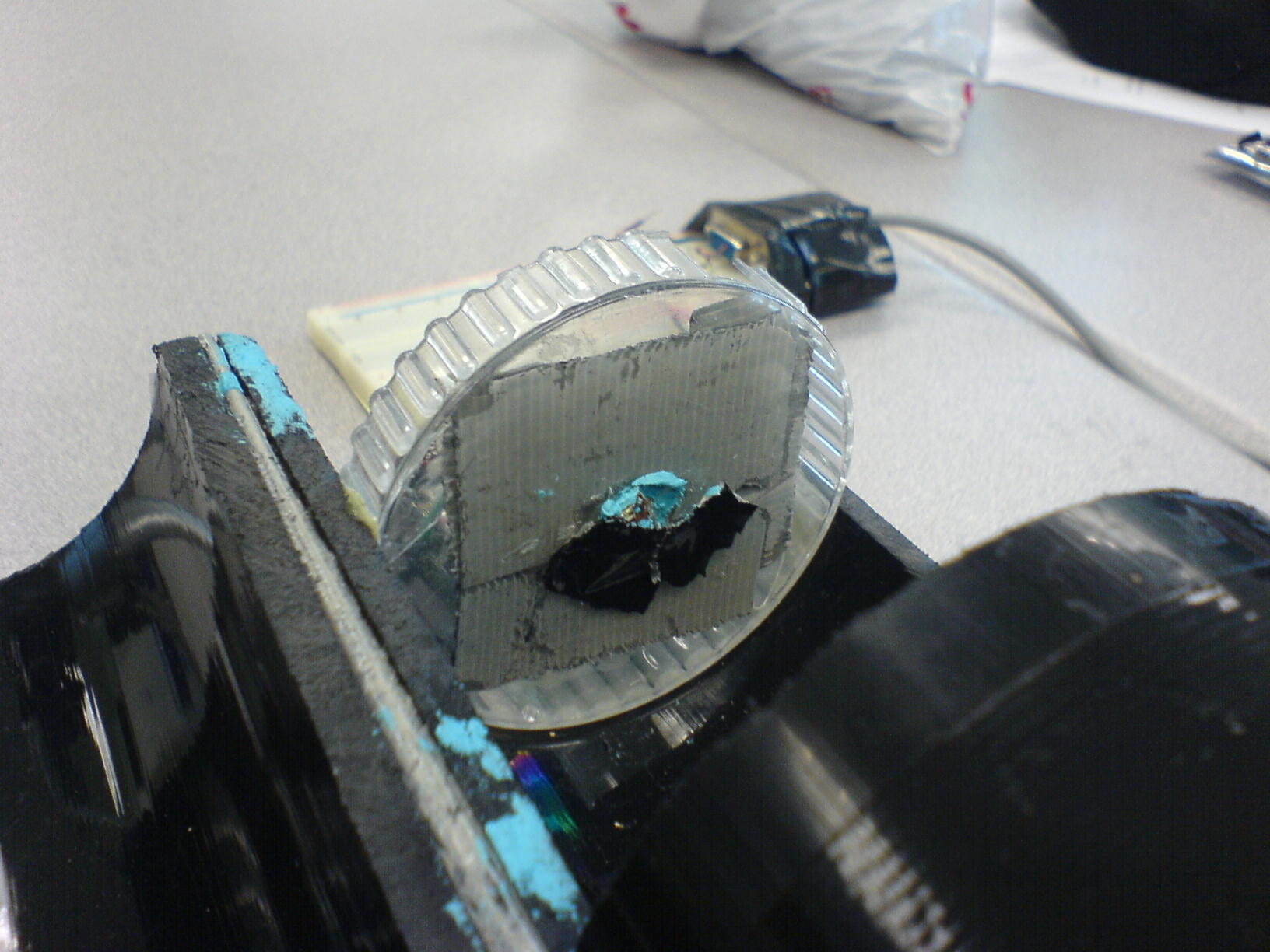
The transistor is of the surface-mount type, which somewhat complicates the mounting process. In order to use it outside of a PCB, external leads must be soldered on to the small contact patches on the collector and emitter of the device. Assistance with this part of the design was provided by lab technician Glen Leinweber. Another unfortunate feature of the device is its very small active area and lack of an integrated lens, which complicates the process of aligning the laser. Nevertheless, the RPM-075PT was found to be an acceptable solution under the test conditions. Here is a close-up of the phototransistor in its mount.
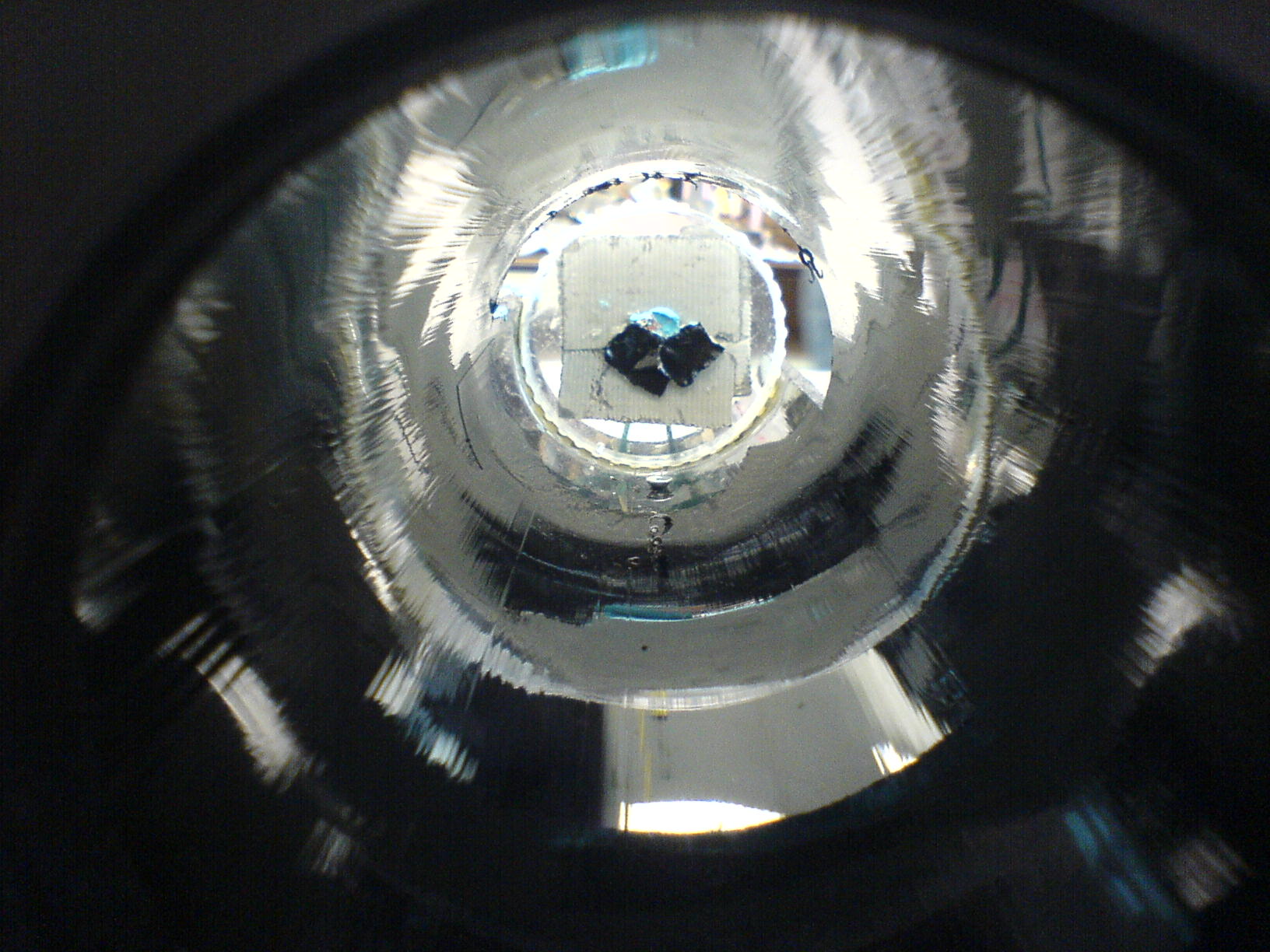
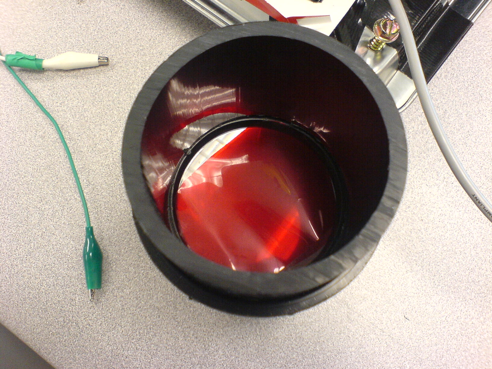
To prevent ambient light from reaching the phototransistor and generating noise, the phototransistor and lens were mounted inside a length of ABS pipe. A piece of transparent red plastic taped over the lens is used as an optical filter, further reducing the amount of noise, since ambient light outdoors is primarily in the blue and green regions of the spectrum. Here are pictures of the mounting and the lens with its filter.
Electrical Design
Group 3 would like to thank lab technician Glen Leinweber for his valuable assistance in the design of the transceiver circuits.
In order to interface between the computer, which sends electrical signals, and an optical communication channel, transceiver electronics are required. In the case of a half-duplex system such as this one, one computer needs to be able to transmit data using the laser, and the other must be able to receive and recognize data based on the phototransistor signals. The group decided to use the computer's serial port interface (RS-232 standard) due to the software and electronic simplicity of communications via the serial port. The maximum speed of ordinary RS-232 serial communication is 115.2 kilobits per second, which is sufficient to send text or smaller pictures in a reasonable amount of time. The transceiver was designed with this data-rate in mind.
The serial port uses a protocol called UART (Universal Asynchronous Receiver Transmitter). In this protocol, a byte of data (8 bits) is represented as 10 bits: a start bit, 8 data bits, and a stop bit. Each bit (a binary 0 or 1) is represented as either a high or low logic level voltage on the TX (transmit) pin of the RS-232 connector. The logic levels for RS-232 are +11.6 V high and -11.6 V low, but in practice the receive (RX) pin will recognize much lower swing voltages of +/- 9 V or less. The signal that must be sent using the laser is an alternating train of positive and negative voltages, with variable-length gaps between 10-bit pulse trains. Since each bit is either a high or low state, a single period of the square wave contains two bits, and the maximum frequency of the transmission can be approximated as being half of the bit rate, or 50-60 kHz.
The design encodes data using a basic on-off keying (OOK) method. High and low voltages from the RS-232 cable are represented by turning the laser on or off. Since the TX pin idles at low logic level (about -12 V), it was decided that a logic low would correspond to the laser being on. This means that the laser will be on when no data is being sent, simplifying physical alignment of the laser and detector. A logic high turns off the laser, causing a change in the phototransistor current that can be interpreted by the receive circuit.
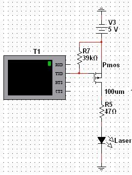
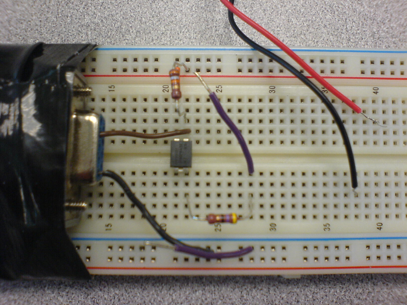
Ordinary laser diodes such as the one being used operate on about 30-40 mA at 4.5 V, and the voltage can be applied in only one direction. The output of the serial cable, which switches between +/- 12 V and operates at a very low level of current, is therefore not suitable to drive the laser directly. The transmitter circuit is built on a breadboard, and consists of an IRFD9010 P-channel power MOSFET, a 47-ohm current limiting resistor, a 39k-ohm gate resistor, 3 AA batteries in a battery holder to provide a 4.5-5 V supply, and of course, the laser itself. Below are a circuit diagram and picture of the transmit circuit.
The P-channel MOSFET is “on” (drain-source channel acts as a short) when its gate is pulled low relative to the source. In this circuit, the source is connected directly to the 5 V rail, and the TX pin of the DB9 RS-232 cable (Pin 2) is connected to the gate. A low logic voltage from the TX pin turns the transistor on, opening the circuit and allowing current to flow through the channel and then through the laser to ground. When the gate is pulled high relative to the source (such as by a +12 V RS-232 high), the MOSFET is “off”, and acts as an open circuit. This prevents current from the batteries from flowing and turns the laser off. Pin 5 (ground) of the DB9 cable is connected to the negative (0 V) terminal of the batteries to establish a common ground between the circuit and the cable.
A 47-ohm resistor in series with the laser dissipates some power, limits current, and reduces voltage at the laser, prolonging the life of the diode. This is especially necessary with battery power; 3 new AA batteries can provide up to 5.5 V, which was found to quickly wear out a cheap laser diode. The 39k-ohm gate resistor prevents static discharge damage to the gate of the MOSFET by providing a path for excess negative charge on the gate to flow to the positive terminal of the battery. Because the gate resistor has a large value, the MOSFET gate is only weakly pulled toward +5 V. This is so external sources such as the cable's TX pin can change the gate voltage.
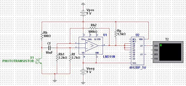
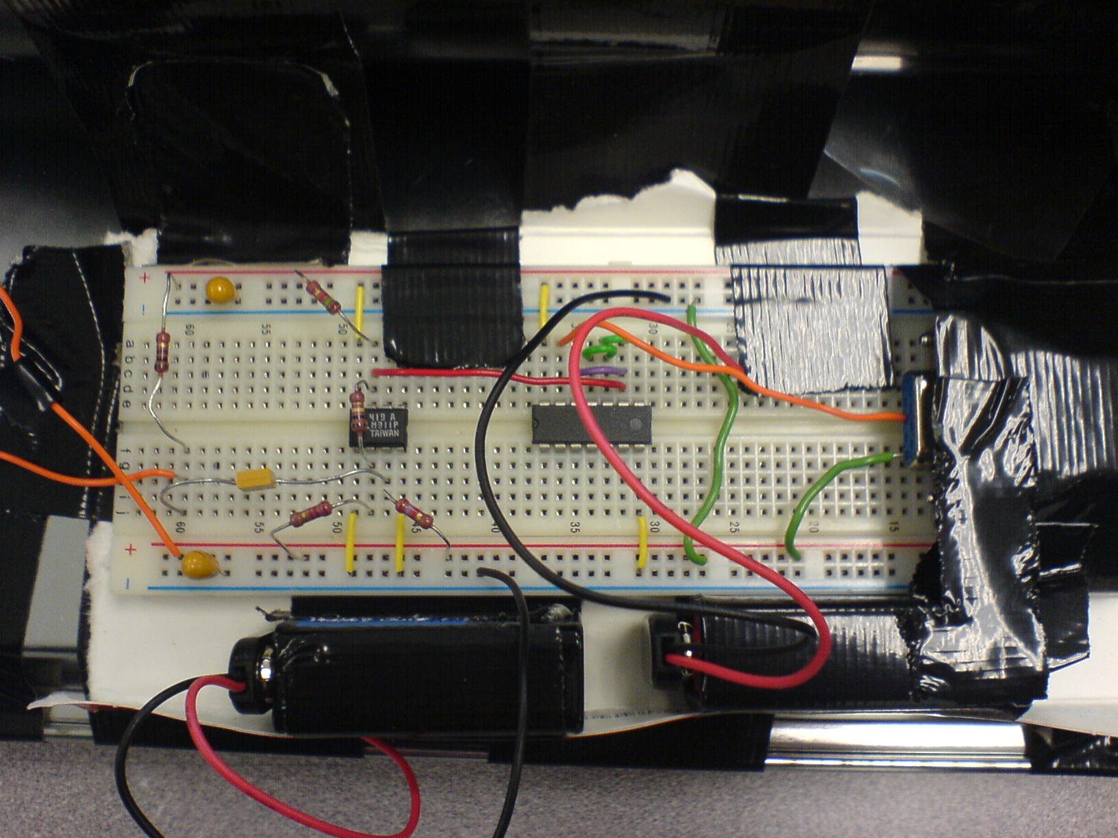
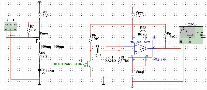
The task of the receive circuit is somewhat more complicated. The receive circuit must take the presence or absence of photocurrent through the phototransistor and convert it back into the +/- 12 V logic levels corresponding to the original transmission. Actually, owing to the much easier availability of 9 V batteries, the circuit outputs a +/- 9 V logic signal instead. As mentioned earlier, this is sufficient to be recognized by the serial port as valid data. A diagram and picture of the receiving circuit are shown below.
Two 9 V batteries are used to provide power and +/- 9 V levels. The upper positive rail of the breadboard is at +9 V. The upper negative and lower positive rails are connected together and are at 0 V. The lower negative rail is at -9 V. The two batteries are effectively in series, with the point between the two being used to provide a 0 V reference.
The sensor must be provided power using a biasing circuit (at left in picture). The emitter is connected directly to ground, and the collector is connected through a bias resistor (Rb) to the positive (+9 V) rail. The value of this resistor is important; since the phototransistor acts as a current source, a larger resistance produces a greater voltage shift in response to light, but also lengthens the response time. Due to the high optical power of the lens-focused laser beam and the sensitivity of the RPM-075PT, even a small 100-ohm resistor can produce up to 4-V peak-to-peak voltage swing between laser on and off levels at the collector, which is a very large signal. According to the transistor datasheet, the rise or fall time with 100 ohms is about 10 microseconds. Since the up-down period of a 60 kHz signal is about 17 microseconds, it proved necessary to use the second-highest (56 kbps, or 28 kHz) data rate to avoid inter-symbol interference and lost bits.
Next, it is necessary to convert the alternating 8.5/4.5 V level at the collector output to RS-232 logic levels. This is accomplished using a comparator. The signal is compared against a reference level, and the comparator “decides” to switch its output high or low depending on which voltage is higher. The LM311 comparator used in the design has an open-collector output, so when the inverting input (the signal, or pin 3) is lower than the non-inverting input (the reference, or pin 2), the comparator is an open circuit, and the collector output (pin 7) is pulled high to +9 V. If pin 3 is higher than pin 2, the comparator becomes a short-circuit to -9 V. Pin 1 (emitter output) is connected to -9 V rather than ground so the output will switch low to -9 V. To avoid short-circuiting the source through the comparator output, a pull-up resistor (Rp, 1.5k-ohms) is connected between pin 7 (collector output) and the +9 V rail. The value of the pull-up resistor was chosen to keep the current to a reasonable level; 18 V dropping across 1.5k-ohm produces 12 mA of current, which is safe for the comparator.
The reference level (pin 2) is provided by AC-coupling the collector output. Capacitor Cf (10 nF) and resistor Rf (2.7k-ohm) form a simple high-pass RC filter, with a cutoff frequency selected to be well below the 28 kHz operating frequency at about 5.9 kHz. The capacitor blocks out the DC component of the collector voltage waveform, changing it from 8.5/4.5 V oscillation to about +2/-2 V oscillations. The output of the filter is connected to the pin 3 inverting input of the LM311. Since the oscillations of the voltage are now centered at 0 V, we can simply reference pin 2 (non-inverting input) to ground to provide a decision threshold, and a -2 V comparator input (laser on) produces a +9 V output.
If the circuit were operating continuously, we could simply connect pin 2 to ground directly. But there are periods (such as during alignment, or when no data is being sent) when the collector voltage is fairly constant. In this situation, Cf discharges through Rf to ground, and the comparator input (pin 3) becomes 0 V. Since the reference input (pin 2) is also at 0 V, the comparator becomes “confused”, switching rapidly between high and low with the small fluctuations in the inputs. The design resolves this using a simple hysteresis implemented using two resistors, Rh1 and Rh2.
Rh1 and Rh2 cause the reference level (pin 2) to shift depending on the output state (pin 7). Since Rh2 is connected between the output and pin 2, and Rh1 between pin 2 and ground, the voltage at the reference pin 2 will be related to the output voltage by the ratio Rh1/Rh2. The input signal swing is about +/- 2 V, and the output swing is +/- 9 V. Rh1 (2.2k) was chosen to be about 50 times smaller than Rh2 (100k), providing around 0.2 V (9*2.2/100) of hysteresis. When the laser first strikes the phototransistor, it generates a current and the collector voltage drops. This causes pin 3 to go down to about -2 V, and the output switches high. This sets the reference to be +0.2 V (1/50 of the output). Thus, when Cf on pin 3 drains to 0 V, the output will stay high, since 0 V is still well below 0.2 V. When the laser turns off at the start of a transmission, the collector voltage goes up to 8.5 V and pin 3 goes to +2 V, exceeding the reference level and switching the output low.
The second integrated circuit is a dual 4-input NAND gate MCP14012 being used as an inverter. With the laser on, the comparator output will normally idle high because of the hysteresis voltage. This is undesirable, as since the TX pin on a DB9 cable idles low, the RX pin expects to see a low logic level when no data is being sent. This also means that the comparator output is inverted relative to the original signal. To resolve this, the comparator output is connected to the 4 inputs of one of the MCP14012's NAND gates. The gate logic causes the output to switch low when all 4 inputs are high, and otherwise switch high. So the comparator output is inverted by the NAND gate and connected to pin 3 (RX) of the RS-232 cable. As with the transmitter circuit, pin 5 (ground) of the cable is connected to circuit ground, to establish common ground between the circuit and the computer.
Note that although the RS-232 cables being used in the project have 9 pins, only 2 are actually connected to either the transmit or receive circuit. The other 7 pins are used for hardware handshaking in serial communications. Since it is impractical to build a system with 8 lasers and receiver just to implement hardware handshaking, the handshaking must be turned off when using the system. Fortunately, most terminal software includes an option to “Remove Hardware Flow Control”, which causes the computer to ignore the levels on the handshaking pins and simply “assume” there is a connection.
4.Proof of Principle
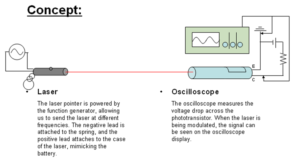
The first and second proof of principle tests performed were intended to test the feasibility of the optical and electrical components of the project, respectively. Below are concept diagrams and explanations of the first (optical) and second (electrical) tests.
Optical Proof of Principle
The optical test proved that the optical sending and receiving components could be modulated/respond to signals at frequencies high enough to transmit data(the tested speed was 50kHZ). The test was attempted inside over a distance of around 8m. The proof had been completed prior to the day of testing, however, due to the unforeseen failure of three laser pointers, the test had to be completed by using a LED to show that the receiver had the capability to respond at the speed required. A different laser had to be used to prove detection because of the lack of a functioning laser which could modulate. The different laser was modulated at a slower speed and detected at a lower speed which proved the principle for the transmission end. These together proved transmission and detection. The source and resistor connected to the phototransistor represent an early version of the biasing circuit.
Electrical Proof of Principle
The electronic test was an evaluation of what eventually became the entire transceiver circuit, excepting the inverter and computer interface components. Instead, a function generator was used to “transmit” and the output of the receive circuit was monitored using an oscilloscope. The circuit designed for the test proved that a digital signal imitating a UART transmission could be obtained from the analog output of the phototransistor. This was completed with a comparator with hysteresis and an RC High Pass filter in front of it. The test was completed without the use of a microcontroller which greatly simplified the task. The day of testing went well and the group successfully obtained digital outputs from analog signals. At this stage both the transmit and receive circuits were being powered using lab DC power supplies .
5.Completed Product
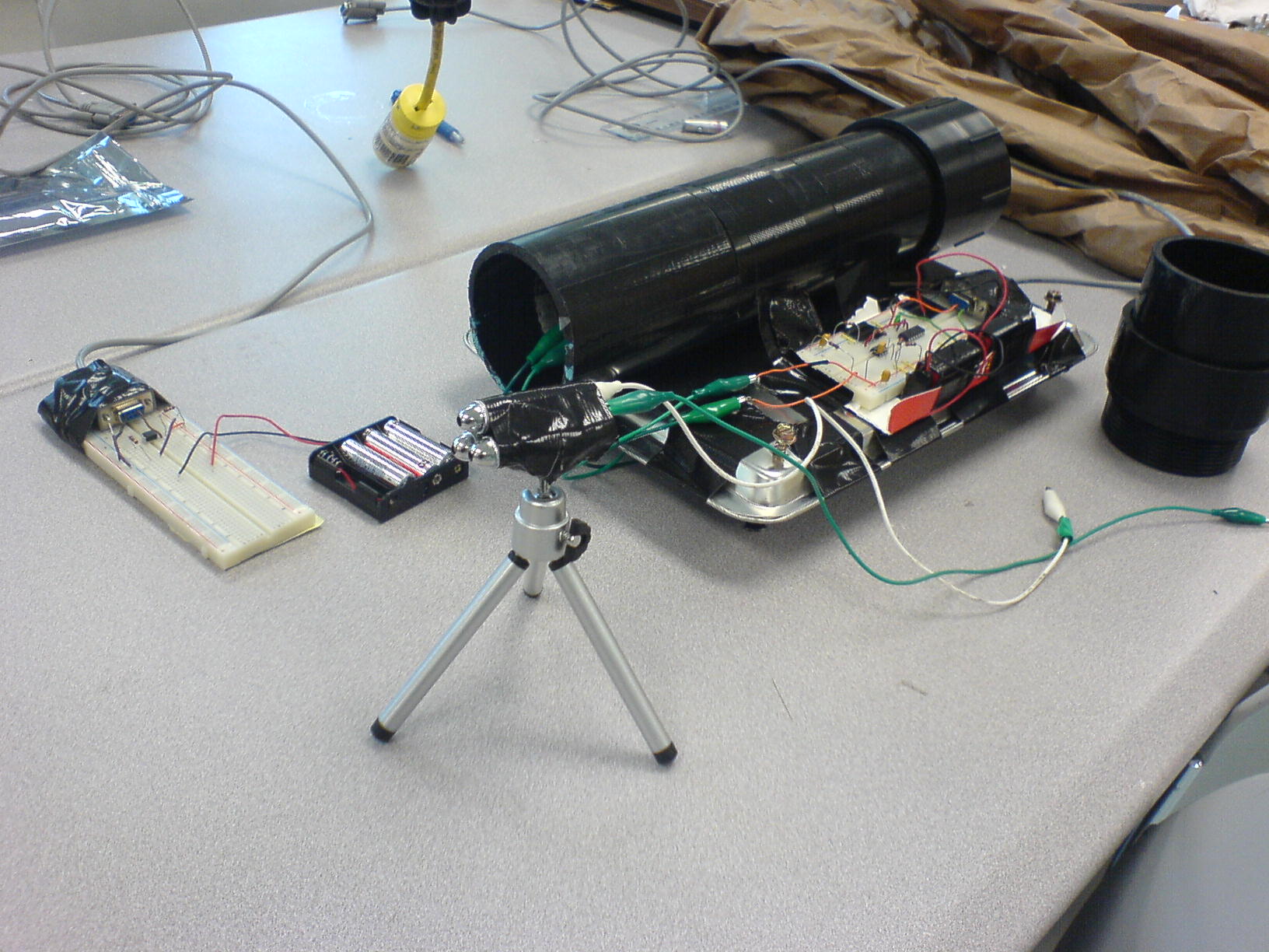
The completed product can be seen below, or, in more detail, in the photos above. The parts list for components used is contained in the budget list. The important and critical devices involved include the laser, batteries to supply power, the p channel MOSFET, the computers with serial cables, the Mounting and aligning equipment, the Tube and filter for noise reduction, the lens for focusing the light, the AC filter for signal isolation, the Comparator for Analog to Digital conversion, and the Inverter for inverting the signal. The total cost for construction is a theoretical $63.90.
Close-ups of some of the components are shown below.
Transmit Circuit
The computer interfaces to the transmit circuit directly, via the RS-232 cable at left in the picture. The circuit controls the laser through two wires attached to the pair of unconnected purple leads in the photo, and is powered by three AA batteries in series. The negative terminal (spring) of the laser connects to the purple lead going to the negative rail of the board. For a more detailed discussion of the operation of the transmit circuit, see Section 3: Final Design. The 5 V battery power supply is not shown in the picture, but the red and black leads entering the photo from the upper right corner are from the supply and are plugged into the + and - rails of the breadboard during operation.
Laser Mount
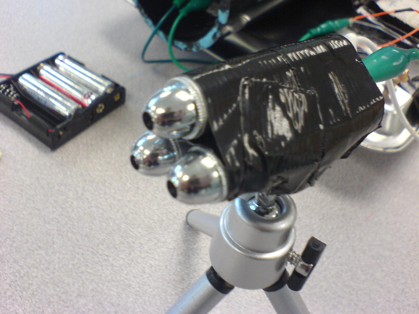
The laser mount is a small tripod intended to be used as a mount for a webcam. The tripods are available for $1 at most dollar stores. Although the laser mount holds three lasers, only one is operating at a given time. The other two are there as spares. All three pointers have been opened and their batteries removed. The two wires are clipped onto the spring (-) and case (+) of the pointer, simulating the contact points of the batteries. Also visible in the background is the 3-battery 5 V supply used for the transmit circuit, made by shorting one of the battery slots of a 4-AA battery holder.
Receiver Housing and Mount
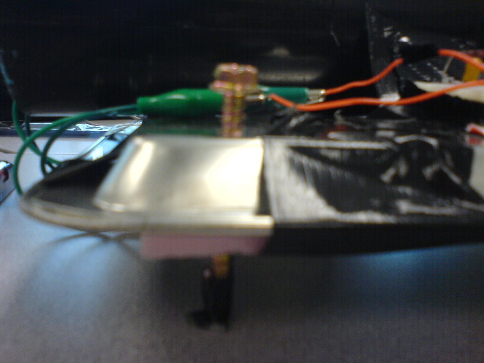
The phototransistor and lens are mounted using plastic cement in a length of 3” ABS pipe. The pipe has a hatch in the rear that can be opened to perform visual alignment of the laser. The pipe is attached using duct tape and a few screws to the baking sheet being used as a receiver mount. The baking sheet has four large screws at its corners, mounted using blocks of styrofoam underneath the baking sheet, that can be used to control height and tilt the receiver during alignment. For all the duct tape, the alignment system is fairly solid and can be used to make quite precise adjustments to the position of the laser spot. For further discussion of the optical components of the system, see Section 3: Final Design.
Receive Circuit
The receive circuit interfaces to the computer directly, via the RS-232 cable at right in the picture. The phototransistor interfaces to the circuit by attaching connecting wires with gator clips to the orange leads on the biasing circuit (at left in the picture). One of the leads is flagged with electrical tape to identify that this is where the transistor's emitter should be connected. The receive circuit is powered by two 9 V batteries, at bottom in the picture. For a more detailed discussion of the operation of the receive circuit, see Section 3: Final Design.
6.Demonstration and Evaluation
The Demonstration and Evaluation of the project was done over two testing days. The first was an indoors test, and the second was an outdoors test. On both days, the test was a complete success. For the indoor test, the alignment was fast and the project worked right away and only malfunctioned when people walked across the beam during transmission of a file. When this occurred, the photo sent would contain Grey rows where information was lost. For the outdoors test, the alignment was more difficult due to low temperature conditions. The beam spot was also difficult to see due to the failure of 2 lasers the day before the test and the use of a high divergence laser on the day of testing. Nevertheless, the alignment was completed and the project worked again despite the higher amount of background light. This proved that the tube and the red filter were sufficient for blocking light.
7.Budget
Parts purchased for the project:
*There is a correction to this list. The quantity of AA batteries bought at dollarama is 1 less than listed. There is also an addition to the list for a tripod used in laser mounting. The cost of the tripod was 1 dollar and it was purchased at Dollarama with the other products. There is no change in the final figures. Also, as a note, the vendor “Home” refers to “Home Hardware”.
Parts used but not purchased:
Additionally, there was a shipping cost of $2.67 for the Digikey order, and a shipping cost of $4.00 for the Newark order. Therefore, the total cost of the project would then be:
Total Cost: $141.31
The cost to construct the system is a different matter, where only the parts used are included. Essentially the figure is an estimation of the cost to reconstruct the system on a mass scale. Also, shipping costs from Digikey and Newark would not be included, since many sets of parts could be purchased at the same shipping cost.
Cost to Construct: $63.90
You are here: start » group3 » group3final
